Programmable LED Dimmer

Around one and a half years ago I’ve designed and built various LED dimmers for both white and RGB LEDs.  Then late last year someone approached me asking if I could make an RGB dimmer for him, too. But my designs were really tailored to their specific applications and built with home-made, i.e. milled PCBs which are time-consuming to make. So I decided to make a more universal version based on a proper, etched board which could be built in a small series and used for all kind of applications, both white and RGB. The result is this versatile, programmable 4-channel dimmer.

The design is based on my previous RGB dimmer but with a number of improvements.

soldernerd.com is now on YouTube

I’ve just uploaded a short video showing this device in action. Here’s the link: https://www.youtube.com/watch?v=ehZybd3Y2kc. This is only my second video so don’t expect miracles but I’d be interested to hear if you would like to see more videos in the future or if you prefer the traditional text and photos format.

Wide voltage range

It now operates from any voltage in the range of 6 to 26 volts as opposed to 12V only. In order to accomodate such a wide range of inupt voltages the regulated logic level voltage of 5V rather than the inupt voltage is now used to drive the mosfets.

Extremely low standby current

This 5V rail is generated by an LM2936 linear regulator with a very low quiscent current and shutdown input. That allows for a nice power saving feature for when all the outputs are off. After a few seconds of sitting idle the entire device powers itself off, i.e. it turns off the LM2936 thus only consuming 30 microamps (typ.) plus some leakage in the capacitors. So the device can stay connected to a battery for months without draining it. To wake it up one has to press any of the two push buttons.

Rotary encoder design options

Talking of push buttons. Like my previous RGB dimmer it features two rotary encoders with push buttons.

But now there are two different types of encoders that can be used.
The ones previously used with their axis perpendicular to the board and a different type where the rotary axis is parallel to the board.
And either type can be mounted on either side which gives you even more freedom for your physical design.

Perfectly debounced switch signals

As always with my designs, the signals from the encoders (six in total) are nicely debounced in hardware by running the RC-filtered signal through a 74HC14 schmitt-triggered hex inverter. So the singals are perfectly clean when they reach the microcontroller.

Noise immunity

With my last design I had experienced some difficulties with ground bounce or insufficient ground connections in general leading to less-than-reliable encoder readings. It’s always more difficult go ensure good, low impedance ground connections on those prototype boards since there are no plated-through holes and vias. On that prototype board the issue was solved by soldering in a few short pieces of wire where the ground connection needed improvement.

So with this new design I paid very close attention to ground. I spent a lot of time working on the board layout to ensure that everything is as noise immune as possible. I always use ground vias generously but here I really tried everything to get the best, shortest and lowest impedence ground connections could get. I’ve also used decoupling capacitors even more lavishly than I usually do.

New microcontroller

I’ve changed the microcontroller to a PIC16F18325 which is smaller and cheaper than the previously used PIC16F1936.
The 18325 has become my standard choicer whenever I need a low pin-count microcontroller. I particularly like its remappable pins which give a lot of freedom to simplify your signal routing on the PCB.

Smaller size and more outputs

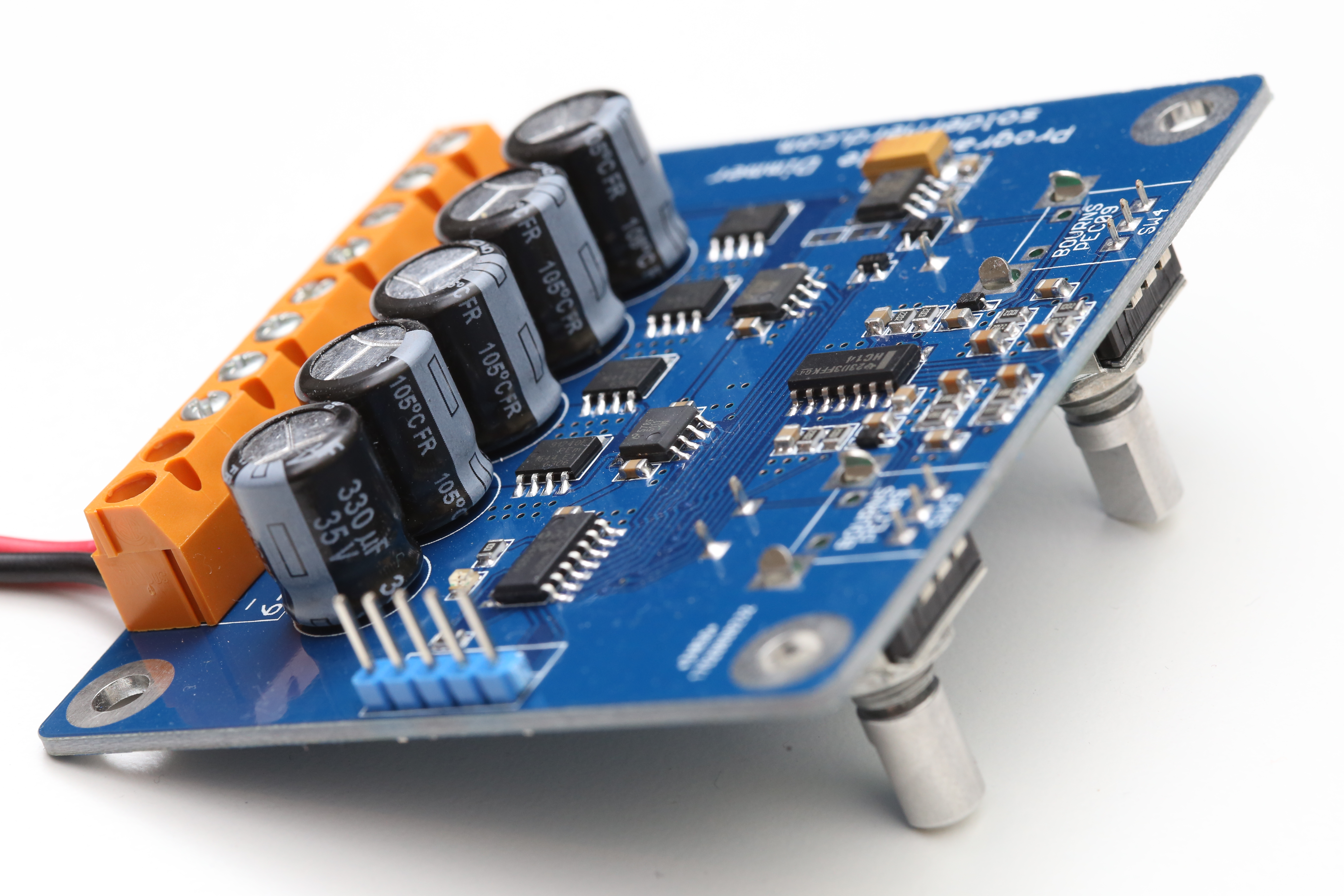
The mosfet drivers are basically the same as before but now with non-inverting outputs: LM5111-1M. There are two of them for a total of 4 outputs compared to only 3 with the previous version.
They now drive much (physically) smaller but no less capable mosfets which allowed me to significantly downsize the whole board to 75x65mm.  The NXP BUK9Y12-40E are rated at 40 volts and offer an on-resistance of 12 milliohms (max @ 25 degrees ) with a 5V drive as we have here. Their large thermal pads a the bottom (NXP calls that package LFPAK) pass heat efficiently to the PCB which then serves as a heat sink. There is also a 30V version that offers even better performance but with a maximum input voltage of 26 volts I thought the 40V version is the safer choice.

As you can see, there’s plenty of capacity on the board. A total of 5 330uF 35V low ESR capacitors are placed in parallel in order to smooth out the PWMs inherent current ripple.

Software

So now we have a device with 2 rotary encoders and 4 outputs but it won’t do anything without software. There’s absolutely nothing hard-wired between the encoders and the outputs so we can program this device to behave in any way we like. That’s what makes it so flexible.

I have so far implemented two functions. The first is aimed at RGB LEDs and behaves exactly like my RGB dimmer. One encoder controls the brightness, pressing its button turns the outputs on and off. The other encoder controls the color, pressing its button toggles between white and color. The three outputs are 120 degrees out-of-phase which presents a more steady load to the power supply.

The second function is aimed at plain white LEDs. There are two pairs of outputs with output 1 & 2 forming a group and 3 & 4 the other. Each pair is controlled by one encoder. Turn it to control the brightness and press its button to turn the respective output pair on and off. The two outputs of any group are 180 degrees out-of-phase to smoothen the load. And since there is a 4th output it is easy to implement a case where there is an independent white channel.

With both functions, the entire device turns off after a pre-defined period of time (currently set at 3000ms) with all outputs off in order to save power. Before turning its own power supply off and hence losing all its data in RAM, the necessary parameters are saved to EEPROM. So the device remembers its last state and will power up the with the same (brightness, color and so on) settings it powered off with.

The switching frequency is 31.25kHz which is high enough to be entirely inaudible and the 10bit resolution gives you 1023 levels to finely control the brightness down to very low levels.

All the settings reside in a file named config.h. That is where you define the function you want the device to perform. The number of brightness levels and their respective values can simply be parameterized there. The same is true for the colors. You can also set the RGB values for neutral white. The seemingly obvious choice of 1023/1023/1023 often does not result in a pleasent white. For my LEDs I had to substantially reduce the green content but this, of course, depends on your particular choice of LEDs.

I currently have 3 devices productively deployed and they perform very nicely. Also, adding new functions is easy since all the heavy lifting like has already been done. It takes somethign like 100 lines of relatively simple code to implement a new function. No need to get involved with any registers and the like. So if you have any experience in C you should be totally fine programming this thing.

Visit github for code and Eagle files

Both the eagle files (including Gerbers) and code are on github:

Also want one?

I have some boards left and can make one for you, too. Fully built, tested and programmed to your needs. Cost is USD 65 payable via PayPal, including worldwide shipping. Simply contact me using this form.

Beacon Keyer

This is likely the first ham radio related project that I document here on this blog. But my very first PIC project was a beacon keyer that I made for my father, HB9BBD. That was was in 2013. A beacon keyer is a great project to get started with microcontrollers since it’s not much more than a fancy way of blinking an LED.

At that time I didn’t even use Eagle yet and so the layouts were based on a software called Sprint Layout. These were all very simple circuits, all based on a PIC16F688, and therefore perfectly suited for making some of my first homemade PCBs as well. The very early versions like the one in the picture above even used the DIP version of the PIC in a socket. All the resistors and capacitors are 1206 size not 0805 like of my later designs.

In fall last year, HB9MPU asked me if I could make some keyers for his new 10GHz beacon. That was a great oportunity to design a new one from scratch and this is what this post is about.

Requirements

These were the requirements:
– 12V operation
– Open drain outputs, i.e. a transistor to ground
– 2 outputs, one of them inverted

Microcontroller

I decided to use a PIC16F18325 this time. Like the 688 it is a 14-pin PIC but a much more recent addition to the PIC16 family. It’s fully featured with I2C, remappable pins, an onboard voltage reference, plenty of timers and a whole bunch of other features. And it’s widely available a very low price. So I tend to use this PIC whenever I need a low pin count micro somewhere. Like for my fan controller.

Outputs

Instead of using discrete transistors and protection diodes I’ve used a Texas TPL7407. That’s a 7-channel low-side driver, basically 7 mosfets to ground together with an on-board voltage regulator for the gate voltage and protection diodes all in a SOIC16 package. It sinks up to 600mA (with a maximum of 2A total) per channel and operates from 8.5 to 40 volts. Perfect to drive relays, small motors, powerful diodes or just about anything else that doesn’t require that much current. Some of you may be familiar with the ULN2003 which does the same thing but using bipolar transistors (as darlington pairs) instead of mosfets.

Power supply

The power supply is based on a Texas LM2931, basically a rugged LM7805 that operates all the way up to 26 volts and survives up to plus/minus 50V. While the LM2931 is reverse polarity protected, the diodes in the TPL7407 will short any negative input voltage to ground which is obviously a bad idea. I’ve added a 60V, 2A schottky diode at the input so the device is truely reverse protected. Minimum operating voltage of the TPL7407 (after a diode drop)  and maximum operating voltage of the LM2931 result in an input voltage range of the final device of 9 to 26 volts.

Speed control

There’s a small pot on the board that lets you control the speed of the keyer. The PIC measures the wiper voltage with its built-in 10-bit ADC and sets its speed accordingly.

Fan output

As mentioned, the TPL7407 has 7 channels but I only really needed two for the beacon keyer outputs, one normal and the other one inverted. The PIC also has an on-board voltage reference module and a temperature sensor so I decided to use all that functionality to add a fan controller. Beacons often have fans that run constantly even when there’s absolutely no need for cooling such as in winter which only wears out the fan’s bearings.

So the pic also measures the temperature and turns the fan output on and off according to software-defined threshold temperatures. Since the PIC’s temperature module is rather inacurate I’ve added an inexpensive but much more accurate LMT86 analog temperature sensor.

I’ve used 4 TPL7407 channels for the fan output so the current is limited by the total allowable current of 2 amps. Of course, you can also use this output to control a relay and use, for example, a 230V fan.

There are also 3 LEDs on the board so you can immediately see what’s going on.  And just in case you care, the board measures 45x45mm.

As always, programming is done with a PicKit3 or similar via a 100mil in-circuit programming header.

That’s pretty much all that is to say about this little device. As always, I appreciate any feedback and let me know if you need one of these.

And as always, everything from Eagle files to firmware is on Github:

MPPT Solar Charger Rev C – First Test Results

Over the last few weeks I have been quite busy with my MPPT Solar Charger project. I’ve built up a first board and started writing firmware for it. Since the last version was not too different in terms of hardware I was able to re-use most of that code. But I hadn’t even touched on the whole USB stuff back then so there was still a lot of work to do. While the project is still far from being complete I am happy to say that I’ve made quite some progress. Most importantly, the new design seems to work well and so far I haven’t found any mistakes in the board layout. But let’s go through this step by step.

USB

I regularly find USB communication to be the most complex and obscure part of the firmware. That’s why I like to get that working first and then add all the other functionality later. I’ve started with some sample code that Microchip provides for their PIC1846J50 family of chips. That way I was able to get the my board act as a composite HID (Human Interface Device) / MSD (Mass Storage Device) quite quickly. Of course, that demo application doesn’t do anything particularly useful but it provides a solid basis for adding the functionality you need.

At least for the HID I’ve implemented most of that functionality. I can read all the relevant data such as settings, currents, temperatures, voltages and so on over USB. I can also control all the outputs as well as the actual solar charger remotely. More on that later.

On the MSD side there is still lots to be done. The solar charger successfully enumerates as a USB flash drive and you can read and write data from and to it. But that’s really it. The charger doesn’t care about the files you save there and also doesn’t put any data there.

Flash and EEPROM

This brings us to the next topic: Non-volatile memory. There is both a I2C EEPROM as well as a SPI flash on the board. Communication with the EEPROM is fully implemented but currently its only used to save the time and date. The idea is to save all the settings and calibrations on the EEPROM. That shouldn’t be difficult but I haven’t had time for that yet.

The flash also works just as it is supposed to but the chip I chose turned out to be a bad design choice. It can’t do page erase, only entire 16k sectors can be ereased. That makes it difficult to use since you have to temporarily save the sector’s data somewhere when you want to change only part of a sector. We don’t have that much RAM so we have to save that data to flash itself. That can all be done but it’s just a hassle. Apart from that a sector erease takes time. A loooot of time. So I’ll just juse a different chip when I do the next iteration of the board. For now I’ll just use the first 512bytes of each sector. That’s extremely wasteful but will do for now I guess.

Solar Charger

The actual charger circuit hasn’t changed much since the last version so I expected little trouble in getting it to work. However, I managed to confuse the low and high gate pins in firmware and only found that bug days later when I had already done plenty of damage to the board. By the time I found and fixed the problem I had already killed the input current sensor, the ADC, as well as some of the PIC’s output drivers.

So I built up a second board but only with the components required to test the buck. And much to my relief it works. And it works well. I haven’t done any precise measurements yet but it seems at least as efficient as the last version. I had it running at its rated power of 75 without it getting overly hot. As expected, most power dissipation takes place in the coil so the coil did get quite warm but not hot. The FETs heat up a bit due to their proximity to the coil but otherwise don’t care much. My main problem with these tests was to somehow sink the power at the output without overcharging the battery. My home-made dummy load can sink up to 4.5 amps but not for very long before it regulates down to avoid overheating. I had the charger running at around 40 watts for several hours and it only got modestly warm.

Also, the wave forms on the scope look nice and clean. There’s considerably less ringing and overshoot than with the last version. So the improved layout seems to work well. During the tests so far I have turned the charger on and off at least a hundred times, switched from asynchronous to synchronous mode and vice versa and had it running for about 10 hours. I also pushed it all the way up to about 85 watts where the coil starts saturating and the caps have to handle more ripple than they are rated for. I’m happy to report that during all these tests I haven’t killed a single fet nor any other component (once the firmware was ok). I am confident that it will stay this way.

Synchronous bucks are somewhat dangerous in the sense that it is easy to short the input or output to ground when you’re not careful. My solution to this is having rigorously tested functions for turn-on, turn-off, switching mode and changing duty cycle and then rely only on these functions when implementing different MPPT strategies. If these few functions do what they should you can get away with quite a bit of abuse without damaging anything.

What I also noticed during my tests is that the break-even between synchronous and asynchronous mode is somewhere in the region of 1 amp. That’s about twice what it was with the last version and is thanks to the extremely efficient diode that makes asynchronous mode much more efficient.

USB Charger and power outputs

This is something that has changed quite a bit since so I was eager to see how it performs. I haven’t done any detailed tests but I’m very pleased with it so far. It definitely performs better than the last version. In theory, you should be able to simultaneously pull 2 amps from each of the two USB charging ports. I haven’t done that yet but when fast-charging two cell phones (approximately 2 amps judging from the power it pulls from the battery) it stayed surprisingly cool – unlike the last version.

Also no surprise with the 4 power outputs. I had changed the mosfet drivers and mosfets in order to save board area. Apart from that everything works like before. I can still turn off the drivers when none of the outputs is in use in order to preserve power. All works as it should.

Solar Charger App

Of course, all the USB HID functionality is of little use without some software on the other side, i.e. running on a PC. I’ve spent a lot of  time writing my Solar Charger App over the past few weeks and I can say it’s getting pretty good. I has already proved very useful in testing the buck. Since I can monitor and control everything via USB there is no need to have a user interface sitting on top of the board during testing. That means unrestricted access for scope and multimeter probes. And since there’s so much more space on a PC screen than on the little LCD I can display all parameters simultaneously.

The program is written in C#, using my recently published HID utility and WPF .  I’ve tested it on Win7 and Win10 and runs absolutely stable. It also copes well with ultra high resolution displays where everything gets scaled-up in order to still be visible/readable. The screen shot above gives you some idea of its current functionality. Take the efficiency measurement with a grain of salt, though. The measurements are yet to be calibrated.

The code is available on github: github.com/soldernerd/SolarchargerApp. To compile it you need VisualStudio 2015 Community which is available free of charge.

Measurements

Measurements is another important topic. The newly chosen 16-bit ADC works well. Actually, I don’t feel much of a difference to the 18-bit version used previously. Anyway, the measurements are done with 14-bit precision only in order to speed them up.


The readings I get from the two current sensors are surprisingly accurate even without having done any calibration so far. So for now, all measurements have been done with their theoretical (i.e. calculated) multipliers and offsets.

The temperature measurements are done by the PIC directly, using a 2.5V external voltage reference. Both the temperature sensors (one on-board, up to two externally) as well as the voltage reference perform just like they should but I get a lot of noise in my otherwise reasonable measurements. This is quite certainly a software issue. I might not give the PIC’s internal ADC enough time to settle after switching channels or something like that. I’m sure it can and will be solved but I haven’t given this very high priority so far.

Next steps

A lot of work remains to be done. One of the next things I will do is to implement proper calibration for the voltage and current measurements. At the moment, all the relevant constants are hard-coded so I first need to change them being variables, store them in EEPROM and retrieve them from there at startup. In a second step I need to make them accessible over USB. Once that’s done it should be possible to calibrate them in a fully automated fashion. I’ve never done that so far but my multimeter as well as my power supplies can be controlled via USB (or GPIB, respectively).  So I want to write a calibration routine that sweeps the device under test, calculates the proper calibration values and sends them to the solar charger.

Getting the Mass Storage Device working from FLASH is another big thing to do. As reported, the currently 7kb of memory on the flash drive are mapped into the PIC’s internal flash memory. I’ll have to dive quite deep into the Microchip USB code in order to figure out how to change that. I expect to spend a significant amount of time until that works but there’s no way around it in the long run.

Once mass storage works properly I can also start implementing settings as a configuration file on the flash drive. So as an alternative to doing things via HID which requires dedicated software to run on the PC you can also check and change settings by editing a text file residing on the flash drive. The next step will then be to also write measured data to that storage.

Then most of the low-power features are still to be implemented. The most basic stuff is there: The 5V buck for USB charging is turned off when not in use and so are the mosfet drivers for the power outputs and the solar charger. The user interface is also turned off after a certain time of inactivity. But the PIC constantly runs at 48MHz, the USB module is never turned off even when not in use, it never goes into any of the several low-power modes and so on. So at the moment it consumes around 10mA with the display off and 16mA with the display on.

And yes, there’s also more testing to be done on a lot of aspects. The code could definitely use a clean-up once I’m done with it, I also have plans of adding a boot-loader so users can update the firmware via USB… I won’t run out of work any time soon.

The firmware is on github, too: github.com/soldernerd/SolarChargerRevC_Software. It is updated much more frequently than I do posts here so if you’re interested I suggest you track the most recent development there.

The next post on this topic is here.