MPPT Solar Charger Design

I’m currently waiting for the boards for my Ultrasonic Anemometer Rev B to arrive from Hong Kong and this gives me some time to write about the MPPT Solar Charger design that I did quite some time ago. I published a series of posts on a Arduino MPPT Solar Charger Shield and got a lot of encouraging feedback. But that shield was more of a proof-of-concept than a finished product.  While it generally performed well it drew way too much current when idle to actually be deployed unless you can count on plenty of sunshine every day.

SolarChargerEagleTop

Aiming for very low power consumption

While I like the Arduino platform I had to admit that it’s probably not ideal for a low-power design. Yes there are some things you can do to reduce the 50mA or the Arduino draws but it will never be truely low power. So I designed a stand alone version with plenty of extra features that I hope to draw only a small fraction of the current. I particularly care about the idle current, i.e. the current it pulls when the solar panel is not producing any energy. In winter, the panel might be covered by snow for weeks and you don’t want your charger to drain the battery during that time. With this new design I’m aiming for an idle current in the tens of microamps. Even if it ends up being 100 microamps that is still 500 times less than an Arduino uses just by itself. And that means it draws less than 1Ah (ampere-hour) per year so you will never drain the battery no matter how little sunshine there is.

SolarChargerSchematic1

PIC18 series microcontroller

At the core of the design is a PIC18F26J50 in a 28 pin SOIC package. It’s capable of running at down to 2.15 volts and consumes extremely little power when running at lower clock speeds. And apart from that it features USB so we can have all the benefits of USB without any external components except, of course, a USB socket.

The PIC has two crystals at its disposal. A 8MHz crystal which will be boosted up to 32MHz by its internal PLL. That’s what the PIC will run on when there is work to do. And then there is a 32.768kHz crystal that will be used to run its real-time clock (RTC). When there is little to no work to do this low-frequency clock will also be used to run the CPU which will greatly reduce power consumption. Power consumption is approximately linear in frequency so this should cut power consumption by a factor of about 1000 compared to full-speed operation.

SolarChargerSchematic2

Switch mode power supply

Now we can run the microcontroller at only a few volts but our power supply is a 12 volt battery. So one of the most straight forward things to do in order to save power was to use a switch mode step-down regulator aka buck.

I looked around and found the Texas TPS62120. It’s only capable of providing 75mA but that’s more than enough for us in this case. It works at a switching frequency of 800kHz and only consumes a bit more than 10 microamps with no load at its output.

It needs a 18uH inductor as well as some ceramic capacitors to work. The output voltage is set via a pair of resistors acting as a voltage divider. I’ve added a n-channel mosfet that allows the PIC to increase the output voltage from 2.2 volts to 3.3 volts when needed. Because while the PIC can run on down to 2.15 volts the display can’t. And even the PIC needs 3.0 to 3.6 volts for USB operation.

Synchronous / asynchronous operation

The actual MPPT converter has changed only little. I’ve changed the mosfet driver to a MIC4605.  Unlike the IR2104 used last time, this model has adaptive dead-time (as opposed to the longish 540ns fixed) and separate inputs for each mosfet. This will allow us to either operate in synchronous (using both mosfets) or asynchronous (only using the upper fet and relying on the diode) mode. Asynchronous operation has a certain efficiency advantage at low power levels so this might come in handy.

The MIC4605 consumes quite little quiescent current for a mosfet driver, only 100uA typical. But that’s still too much for our purpose. So the PIC can power the whole thing off via a NPN transistor and a p-channel mosfet. That BUCK_ON signal also serves as the supply voltage for the INA213 current sensors already used in the last version. So the entire converter can be powered off and should consume precisely zero current when not in use.

What about the voltage divider necessary to measure the battery voltage? That’s been taken care of, too. That divider is interrupted by a (low threshold voltage) n-channel mosfet unless a signal from the PIC turns on the mosfet and closes the circuit.

SolarChargerSchematic3

Port expansion

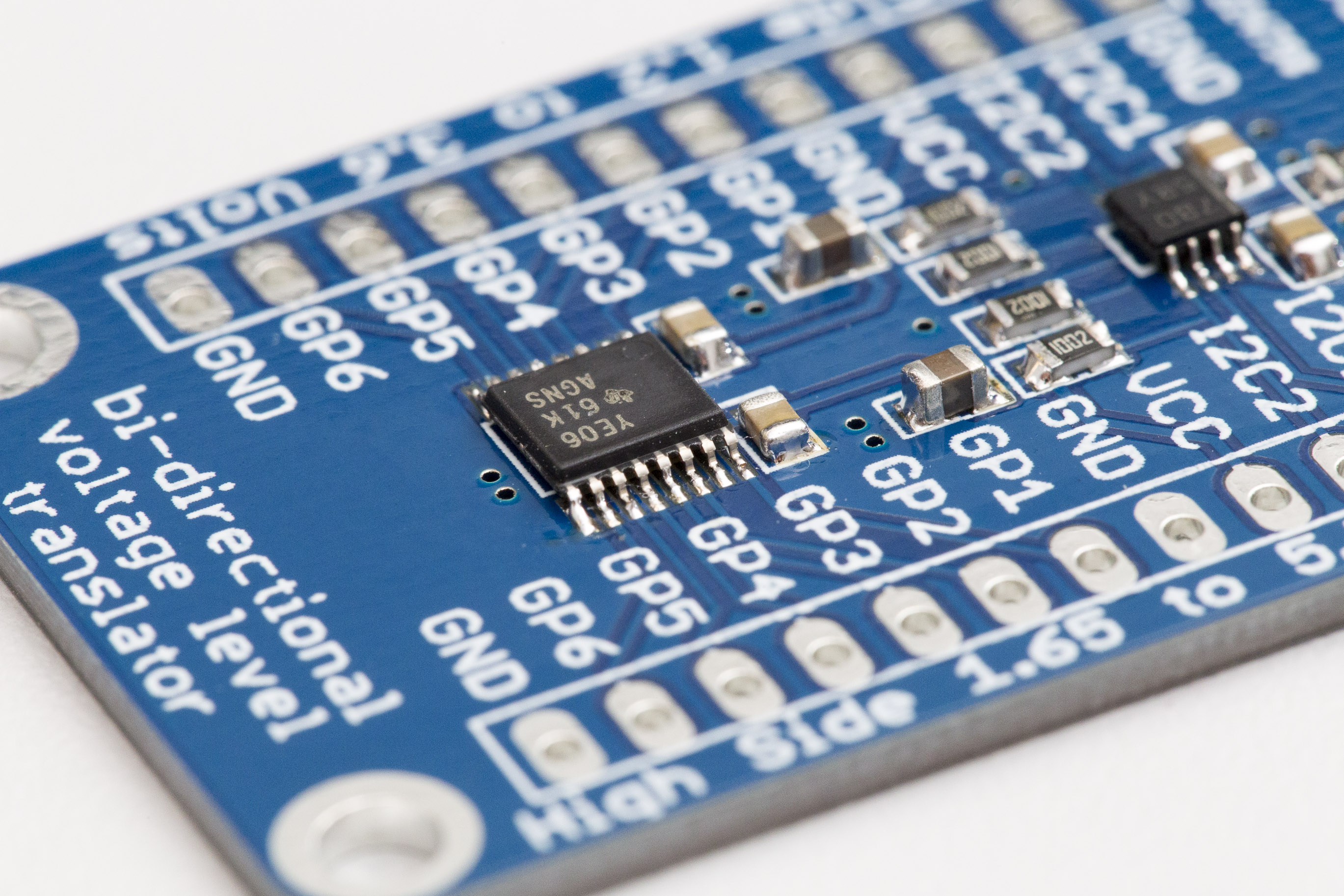
I soon ran out of GPIO pins with that PIC so I had to add an I2C port expander (MCP23008) to gain another 8 I/O pins. I’ve also added a PCA9546 I2C switch in order to translate between different voltage levels.

It’s probably not the most elegant solution and a future version might trade these 3 chips for a higher pin-count PIC. But I had all components here already so that’s what I’ll use for now.

Precise measurements

In order to precisely measure input and output voltages and currents there is now a MCP3424 4-channel 18-bit ADC. To be sure, we don’t need 18 bits of precision here but we’ll trade some of that precision for speed and work with 14 or 16 bits.

The ADC has its on-board voltage reference and PGA with gains up to 8.  Since it only consumes a maximum of 1uA in standby mode it is always powered on.

There are also a total of 3  LMT86 temperature sensors, one on the board and 2 external ones. The external ones are intended to measure the temperature of the panel and battery, respectively. The maximum voltage for a battery is quite dependent on temperature so that’s a useful information to have. The inputs from the temperature sensors are measured directly by the PIC.  For that purpose there’s also a ADR361 2.5V voltage reference.

Measuring temperatures requires the board voltage to be high, 3.3 volts nominally. So both the voltage reference and the temperature sensors are only powered on when then VCC_HIGH signal is set.

User interface

To communicate with a human user there is a 4×20 LCD display that is controlled via I2C in order to save some I/O pins. There are quite a few external components needed to run it at 3.3 volts so it has its own PCB and connects via a 5-pole wire. There is 3.3 volts and ground for power, SCL and SCD for I2C communication and a PWM singal in order to control the display brightness. Because that’s a rather universal board I will document that as a separate post.

As an input device there’s a rotary encoder with push button. Together with the display (and some decent software) that should allow for a pleasant user experience.

The inputs from the encoder are debounced in hardware via a 74HC126 that serves a double purpose. With its 3-state outputs it allows us to use the pins that are otherwise used for in-circuit programming of the PIC.

Both the rotary encoder (except the push button) and the entire display unit can be powered off when not in use. The push button is always powered on so the user can wake up the user interface at any time by pressing the button. When the user interface is not actively powered on the 74HC126’s outputs are in high-impedance mode and the PIC can be programmed without being affected by the rotary encoder.

SolarChargerSchematic4

Data logging

One might be interested how much energy has been harvested by the solar charger over the last hours, days, weeks or months. So there’s some non-volatile storage as well. The 24FC256 connects via I2C and offers 256kBit of memory. It consumes only 100nA in standby so it can stay powered on at all times.

Fan control

As mentioned, there’s a temperature sensor on the board. If it gets too hot, a fan can be powered on via the FAN_ON signal controlling an n-channel mosfet.

Outputs

There are 4 power outputs, each controlled by a separate signal from the PIC. There should be some PWM modules left on the PIC so some (two I think) can be PWM controlled. A typical application would be LED lighting which can be controlled and dimmed directly from the solar charger via the rotary encoder. Each output channel has a beefy  mosfet of the same type as the MPPT switcher (IPB136N08N3).

Each has its own FAN3111E mosfet driver. They have a separate input for the reference voltage so the PIC can easily control them when running at only 2.2 volts. The FAN3111 should only draw 5uA (10uA max) when idle but there are 4 of them so they can be powered off (all togeher, not individually) when not in use.

SolarChargerSchematic5

USB charging ports

One of the first thing one wants to do when there is power is to charge one’s cell phone or similar device. So there are two USB charging ports capable of delivering some 2 amps of current at 5 volts in total.

They are powered from the 12V batter via a TPS54231 buck converter. So there are a total of 3 buck converters on this board… It is always connected to the 12V rail but the PIC can turn it off when not in use. The regulator’s shutdown current consumption is only 1uA typical (4uA max) so that should be adequate.

Manufacturers of mobile devices have all come up with nasty ways of making their devices incompatible with other manufacturer’s chargers. They basically abuse the otherwise unused (for charging purposes) data lines to recognize their own chargers and discriminate against any others. That might mean they won’t charge at all or only at a slow rate.  So there are two charging ports on this board, one emulating an iPad charger and the other one a popular Samsung scheme. So pretty much any device should be able to charge on at least one of these ports at a reasonable speed.

Summary

As you can see, there’s a lot of functionality in this new design just waiting to be unlocked by some clever software.  I’ve already milled a board and I’m looking forward to populating it and bringing it to life. I guess that will be quite a bit of work but I think its well worth it. Thanks to all of you who have kept asking about this project – I very much appreciate all your feedback.

There are only Eagle files (including PDFs of the layout and schematics) at this point. They can be downloaded on the overview page. There’s now also a prototype. First test results are presented here.

Ultrasonic Anemometer Part 26: Rev B Board ordered

I recently ordered my first PCB at dirtypcbs.com and the result was promising. So there was nothing stopping me from finalizing the Rev B of my standalone Ultrasonic Anemometer and ordering a protopack. I’ve placed the order a few days ago and expect the boards to arrive here in 2 to 3 weeks. This should be good news for all those of you who have been asking for kits and want to contribute to the further developement of this project. I’ll build up one or two boards as soon as they get here and do some testing. If everything works as planned I can order some more components and ship some kits soon after that.

EagleSnapshot

So today I’ll go through the changes I’ve made compared to the previous version. All in all the changes are quite minor and only require minimal changes in software. But let’s go through them one by one.

Non-volatile memory

This is the biggest change from a functional point of view. The PIC32MX250 doesn’t have any EEPROM memory of its own. So in order to be able to save some settings an the like I’ve added a Microchip 24AA16 I2C EEPROM providing 16kbit (2kB) of non-volatile memory. That should be more than enough to store any settings and calibrations one might want to make. For example, this gives the user the possibility to calibrate the filter kernels to the transducers used. Of course, the software first needs to make use of that memory but I think it’s great to have the possibility to durably  store a reasonably large amount of data.

dirtypcb_top

Support for 5V I2C communication

I’ve hinted at this in a previous post. On the Rev A board the I2C signals were pulled up to the 3.3 volt rail. This was great as long as one didn’t want to interface to a 5V device such as an Arduino. The microcontroller pins are 5V compatible so you want to be able to pull those lines up to 5V whenever you interface to a 5V device. So I’ve added a diode to allow the SDA and SCL lines to be pulled higher than 3.3 volts. The I2C reference voltage of 3.3 volts minus a schottky diode drop or about 3.1 volts is accessible from the I2C header at the bottom. So just connect that to the external device’s 5V operating voltage and you have a fully compliant 5V I2C bus.

dirtypcb_bottom

Physical layout and connectors

There was a rather large 8-pin connector on the last version to connect to the transducers. Now all the connectors along the edges of the board are standard 100-mil headers. This also allowed me to slightly shrink the physical size of the board to 60x70mm.

The pinout has also slightly changed. The board is now powered from a header on the right-upper side and all three voltage rails are now externally accessible from a newly added header on the right side. The pin order on the I2C and SPI headers on the bottom side of the board has changed, mainly to accomodate an exteral I2C reference voltage.

GerberViewerScreenshot1

Power supply

The tiny (SOT23-5) 3.3 volt linear regulator on the last version worked well but got rather hot when providing close to 50mA from a 12V input voltage. I never had any issues with it at room temperature but decided to be cautious and upgrade to a LD1117 regulator in a much larger SOT223 package. This should be more than sufficient any reasonable ambient temperature..

GerberViewerScreenshot3

Miscellaneous changes

I changed the digipot used to set the amplifier gain to a Microchip MCP4531. This model only has 128 steps but this is still more than sufficient for its task and it’s quite a bit cheaper than the 256-step version.

I also had to change the crystal because the model previously used became unavailable.

GerberViewerScreenshot2

That’s it for now. I’ll let you know as soon as the boards get here.

Bi-Directional Voltage Level Translator – Board House Test

20160706_VoltageLevelTranslator_002

While most of my microcontroller designs run on 3.3 volts there is still the ocasional 5 volt design. Or I do something with an Arduino. So the need may arise to interface between logic working at different voltage levels. There are several ways of doing this, depending on your needs. Things are relatively simple as long as you know in advance which side is transmitting and which side is receiving. It gets more difficult if the communication is bi-directional or with busses such as I2C that are bi-directional by nature. I did a search on farnell.com and identified two chips that can translate between almost any two voltage levels bi-directionally. The Texas Instruments TXB0106 works with up to 6 CMOS (i.e. actively driven high or low) signals for protocols such as SPI. The PCA9306 (also from TI) is intended for protocols such as I2C that rely on pull-up resistors and where a line must never be actively driven high.

20160706_VoltageLevelTranslator_010

I ordered a few of these chips and laid out a simple board that contains the two chips together with the pull-up resistors and some decoupling caps. I also added two larger 10uF ceramic capacitors for a generous amount of bulk capacitance. The result is a tiny little board (45x30mm) that can universally be used to translate between almost any two logic voltages for almost any protocol.

Giving dirtypcbs.com a try

I can think of a lot of situations where it could be useful. But the main reason for this project was to gain some experience with getting a PCB professionally manufactured by a board house. For several years I have done my own designs but I always milled and drilled them myself. This had pros and cons. I never had to worry about silk screens or solder masks because my boards never had any. On the other hand I suffered from the lack of plated-through holes. Vias were always a pain in the arse because I had to manually solder in pieces of wire to connect the two sides. And it was very difficult if not impossible to put a via below a component which made the layout challenging when working with ICs with many and/or tightly spaced pins.

20160706_VoltageLevelTranslator_013

So this simple project seemed perfect to gain some experience in getting a design made by a board house. I chose dirtypcbs.com for their unbeatable prices and read their requirements and restrictions.

20160706_VoltageLevelTranslator_006

Here are some things to watch out for:

  • If you’re working with Eagle you can download a design rule file to automatically check if your design fulfills their requirements. This is great for checking things like minimum via size or trace width/spacing.
  • Make your own gerber files. Yes, you can just send dirtypcbs.com your Eagle files and they will take care of it. But I highly recommend you do it yourself so you know what you’re getting. It’s not difficult. Just download their .cam file and run it. I modified it somewhat so the file names reflect what the file contains. The file types themselves are rather cryptic.
  • View the gerbers online: There are several online gerber viewers available for free. I particularly like the online viewer at mayhewlabs.com. Just drag and drop the gerber files produced in Eagle and get a beautiful 3D view of your design. Check it carefully to be sure the gerbers represent what you are after. My workflow was rather iterative: I produced the gerbers, looked at them online, changed something in Eagle, produced some new gerbers… Again and again until I was happy.
  • Control what’s on your silk screen. A lot of the silk screen comes directly from the component libraries. Typically, the libraries print the outline, orientation, part name and part value on the silk screen. Unless your layout has a loooot of space between components the silk screen will soon be cluttered with all that information. I recommend you make your own libraries. You can then change the components  to only contain the information you want and how you want it. I ended up only putting the outline and orientation of the components on the silk screen.
  • Be aware that the design rule check will not look at your silk screen. You need to make sure your silk screen meets the minimum width of 0.15mm. If you’re using vector fonts (as you should) the math is simple. Just multiply the font size by the font ratio to calculate the line width. Example: A 70mils font size with a 10% ratio gives a line width of 7mils or 0.178mm.
  • Make sure your silk screen doesn’t overlap any of the pads. Again, he design rule check will not check for this. The board house might avoid printing the silk screen over an exposed pad but I wouldn’t bet on it.
  • Eagle seems to do quite a good job with the solder mask without any manual intervention but check the result carefully using the gerber viewer. Pay particular attention to the vias. You generally want your vias to be covered with solder stop – there’s no reason to have them exposed. But you might have some vias that you use as pads to access some signal for testing and debugging. Make sure they are not covered by the solder mask. An easy way to distinguish by the two types of vias is by drill size. You can set this parameter under DRC -> Mask -> Limit.

20160706_VoltageLevelTranslator_020

It took me quite some time until I had my files ready for manufacturing. Especially given the simple nature of this project. I then ordered a proto-pack from dirtypcbs.com. I went for a industry-standard 1.6mm (they default to 1.2mm) FR4 with a cool-looking (and non-standard) blue solder mask at no extra cost. Some 3 weeks later I found 10 of those nice little boards in my mailbox. They are quite precisely how I expected from the gerber viewer. When you look at them close enough you’ll notice that the solder mask and silk screen are not perfectly aligned. The silk screen could also be somewhat cleaner. But don’t get me wrong – I’m not complaining. The quality is absolutely ok, these are nice little boards. And at this price – I paid 14$ including everything – they are simply amazing. Thank you, dirtypcb.

20160706_VoltageLevelTranslator_019

So the board house test was a success but how about the rest? So far I’ve only populated a single board. And while I haven’t actually used it yet I have performed some tests with a signal generator and a scope.

PCA9306 for I2C

So let’s look at the PCA9306′ performance in some more detail.

I2C_50_18_1MHz
I2C: 5V to 1.8V at 1MHz

The chip performs excellently when translating from a high voltage to a lower voltage. In the  example above it is translating from 5 volts to 1.8 volts at a very high 1MHz frequency and the wave forms still look nice.

I2C_18_50_100kHz
I2C: 1.8V to 5.0V at 100kHz

Translating in the opposite direction (1.8 to 5 volts) everything is fine at 100kHz.

I2C_18_50_400kHz
I2C: 1.8V to 5.0V at 400kHz

At 400kHz the output waveform starts to look very jagged, however.

I2C_33_50_400kHz
I2C: 3.3V to 5V at 400kHz

But of course, translating from 1.8 to 5 volts is a rather extreme example. In the much more likely scenario of translating from 3.3 to 5 volts the chip performs reasonably well, even at 400kHz. And I2C doesn’t usually happen at frequencies higher than that. An Arduino, for example, will usually work at 100kHz. So I’m very happy with the performance so far.

TXB0106 for SPI and the like

Now let’s look at the TXB0106.

50_18_100kHz
5V to 1.8V at 100kHz

Translating from 5V to 1.8V at a modest 100kHz is rather undemanding and the waveforms look nothing but perfect.

50_18_1MHz
5V to 1.8V at 1MHz

Even up at 1MHz this translation works totally fine.

18_50_100kHz
1.8V to 5V at 100kHz

Translating the opposite way, from 1.8V to 5V is more demanding but works very well at 100kHz.

18_50_1MHz
1.8V to 5V at 1MHz

However, at 1Mhz the wave forms start to look pretty uggly. And with a protocol like SPI it is much more likely to actually operate at 1MHz. Note that the glitches might be an artefact of my primitive test setup.

33_50_1MHz
3.3V to 5V at 1MHz

As with the other chip, the output signal starts to better when only translating from 3.3 volts to 5 volts. As mentioned above this is a much more likely application and the chip does a decent job even at 1Mhz.

Support this blog – Buy one

By the way: If you need one of these universal voltage level translators you can support this blog by ordering one (fully assembled) for USD 20, including worldwide shipping. Just use the contact form on the about me page.

20160706_VoltageLevelTranslator_004

With the following link you can download the Eagle files as well as the gerbers. Just click here.

Ultrasonic Anemometer Part 25: I2C Interfacing and more

20160706_StandaloneAnemometer_023

It’s been a long six weeks since my last post but that doesn’t mean that I haven’t done anything since. Among other things, I wrote some code to get the I2C interface working and hooked the anemometer up to an Arduino Uno with an LCD display attached. Apart from demonstrating the I2C interface this also nice for testing. For the first time I can see what this thing is measuring in real time without hooking it up to a PC over USB.

20160710_StandaloneAnemometer_025

I2C Interfacing

But let’s look at the setup in some more detail. The PIC has a total of two I2C interfaces and I’ve made both of them accessible via the 100mil headers along the edges of the board. One of them is primarily intended for internal purposes like controlling the gain via the I2C digipot. The other one can then be used to interface to some external logic without having to worry about any internal communication. This external I2C interface also comes with 5V compatible pins which means we can interface to 5V devices like an Arduino without any further logic level translation. All we need is a pair of pull-up resistors pulling the SDA and SCL lines up to 5 volts. The Arduino’s Atmega328 already has built-in (weak) pull-up resistors so that’s not a problem. I didn’t think of interfacing to a 5V device when I designed the board and pulled the I2C signals to the anemometer’s 3.3V supply. So for proper 5V operation I’d have to unsolder the two 10k resistors. Luckily, 3.3 volts is enough to almost certainly be recognized as a logic high by the Arduino so the setup works anyway. But I will think about how to improve this in the next version. I might add a diode to allow the lines to be pulled higher than 3.3 volts.

The I2C interface can be configured to act as a master or as a slave device. For now I’ve only implemented slave mode so the wind meter behaves just like a I2C temperature sensor or external ADC. The Arduino acts as a master and asks the slave for its latest measurement every 250ms. The anemometer then returns 8 bytes of data consisting of 2 status bytes, north-south wind speed, east-west wind speed (both in mm/s as signed 16-bit integers) and temperature (0.01 degrees centigrade as signed 16-bit integer). It’s also possible to send data to the anemometer. That data is then saved to a buffer is otherwise ignored.  In a future version of the software one might use this functionality to set the data format to wind speed and wind direction or to change the temperature unit to kelvin or fahrenheit.

20160710_StandaloneAnemometer_027

It would not be difficult to implement master mode as well but so far I haven’t done it yet. A lot of code could be copied from the module communicating with the digipot where the PIC acts as a master. The anemometer could then push data to an external device whenever a new measurement becomes available. Definitely something I’d like to implement at some point but no priority right now.

Bug fixes

I’ve found (and fixed) a number of bugs while testing. Among other things, the axis and direction signals were not always properly set and so the measurements did not always correspond to the direction they should. So take with a grain of salt some of the test results reported earlier. Some of them were almost a bit too good to be true and this bug might have been the cause. I suspect I might have compared two successive measurements in the same direction when I actually wanted to compare measurements taken in opposite directions. But I’ve fixed the code and I’m confident that now all the directions are set and reported correctly.

Individual filter kernels

EqualAmplitudes

As can easily be seen from the scope screenshots above, the shape of the received signal varies quite a bit from transducer to transducer. Note that the amplifier gain is dynamically adjusted to make sure the peak amplitude is the same for all of them but the shape still differs quite substantially. So the kernel for the matched filter has to be some compromise to suit them all. I have now modified the software to use four individual kernels, one for each direction. This gives us the flexibility to calibrate the kernel to each transducer and so get more reliable results for the absolute phase.

Revised board

20160710_StandaloneAnemometer_026

My main priority at the moment is to complete the revised version of the board and to order a small series of boards. Until recently I never ordered a board from a professional board house so there are quite a few things for me to learn. For the first time I have to worry about silk screen, for example. Or solder mask. On the other hand, a board house can do a lot of things I can’t. Plated-through holes for example. Or smaller vias. Or place vias under an IC. This means a lot more flexibility in my layout that I first have to get used to. But I’m making progress. I got a simple design of mine produced by dirtypcbs.com and got a batch of very usable boards. More on that in a future post.

Wind tunnel

If you’ve been following this project for a long time already you might remember my simplistic wind tunnel made of a 120mm brushless fan and a cardboard tube. I got a number of suggestions from you guys on how to build something better than that and I also found some useful material online. So I’ve started to build a much improved wind tunnel that will hopefully allow me to perform more meaningful tests. That’s also for one or more future posts.

20160706_StandaloneAnemometer_021

Software ideas

I’ve also played around with some software ideas that I believe to have potential. One is dynamically adjusting the frequency. I’m now only working at the transducer’s nominal frequency of 40kHz. But the individual transducer’s resonance frequency might be somewhat different and might change with temperature or age. So I might try to adjust the frequency dynamically using some perturbation and observation algorithm.

I’m also thinking about measuring at two slightly different frequencies (say, 39.5kHz and 40.5kHz) and using the two phase shifts to figure out the absolute time-of-flight. I’ve given it a try and was not very successful but I haven’t given up on that idea yet.

So that’s it for now. The code for the Ultrasonic Anemometer as well as the Arduino are available for download. See the overview page for the respective links.