Today I’ll go through each part of my new Arduino shield to see if it performs as expected.
If you’re new to my Arduino-based ultrasonic wind meter project, you might want to click here for an overview: https://soldernerd.com/arduino-ultrasonic-anemometer/
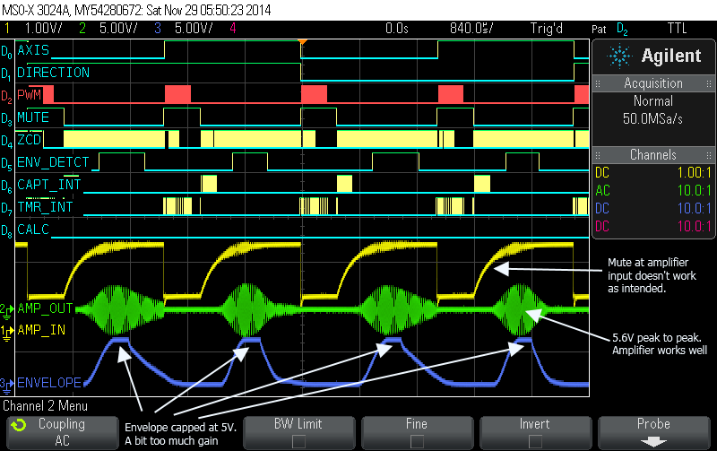
When I first powered on the new shield, only two out of the four transducers worked. As it turned out, I had two different Direction signals on my schematic: one named DIR and one named DIRECTION. They should be one and the same signal but Eagle had no way of knowing about that so they ended up unconnected on the board as well. But luckily it was easy to fix with a piece of wire. After that, the circuit was quite ok. This was the first impression (with some comments of mine):
But let’s go through it step by step.
Amplifier
This was the main design flaw of the first version. Yes, it eventually worked but drew much more current than necessary. This one got the gain right the first time as can be seen from the screenshot above. Output amplitude was about 5.6V pp and the signal looked nice an clean.
So all I had to do was to tune the LC tanks to get them to resonate at 40kHz. The inductor has a 20 or even 30 percent tolerance rating and I can’t measure it. So I had to start somewhere, see how it performs and adjust it from there. I started with a 15nF cap and used a signal generator to find the resonance frequency for each amplifier stage.
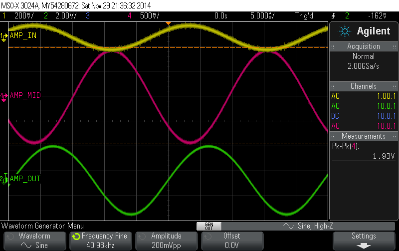
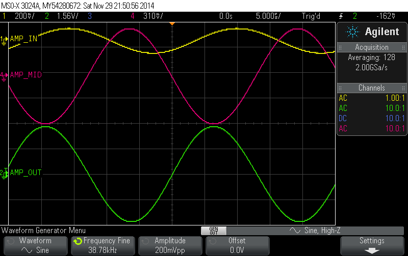
At resonance, the phase shift is exactly 180 degrees. Maximizing gain should give the same result but I found it easier to look at the phase shift. Above you see two screenshots: one with the first amplifier stage in resonance at 40.98kHz and one with the second stage in resonance at 38.78kHz.
From that you can calculate how much more or less capacitance you need. It took me 3 attempts to get it really right but the final result looks like this:
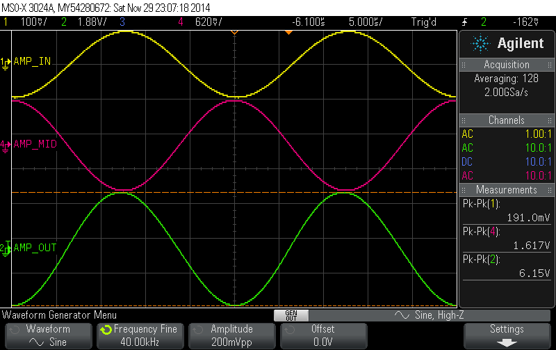
Both stages are perfectly at resonance at 40kHz.
About the biasing: I’ve removed the 10k speed-up resistors R6 and R11. I guess they were unnecessary to start with and they lowered imput impedance too much. I noticed by the fact that there was a noticable voltage drop across the 100k biasing resistors R3 and R4. So while the emitter of the biasing transistor pairs was precisely 1V above ground as intended (I measured 1.015V), the actual amplifier’s darlington pair had it’s emitter only about 0.85V above ground. Not at all what I was looking for.
With the two resistors removed everything is fine. 1V emitter voltage for each of the four darlington pairs. And no measurable voltage drop accross the 100k resistors.
Zero Crossing Detector
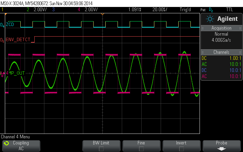
I had changed the comparator to a much faster type and this is the result. Now it triggers exactly at the zero crossing, without any noticable delay.
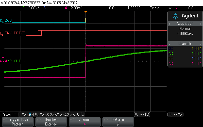
Before it triggered nowhere near the actual zero crossing because it always lagged behind so much. Now this problem is gone and the edges of the ZCD output are very clean and steep. If you zoom in even more you’ll see that rise and fall times are only around 20ns and there is no overshoot and ringing.
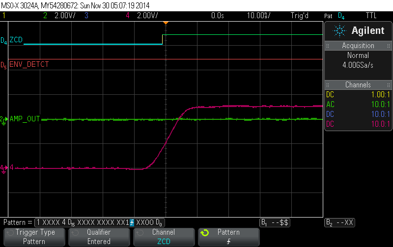
No excuses for the Arduino to not trigger accurately on them.
Envelope detector

I had changed the envelope circuit quite a bit. It has now two op-amp buffered low-pass filters. And this is what I get before the first stage (yellow), after the first stage (pink) and the final envelope (blue).
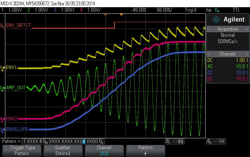
The first buffer has a gain of 2.5 set by the 15k and 10k resistors (R9 and R10). This has caused the op-amp to rail before the maximum amplitude was reached. I thought about reducing the gain but then decided to leave it as it is.
It doesn’t matter if we cut off the top of the envelope. All we care about is the rising edge, this is what we trigger on. We don’t care what happens after that. So the high gain gives us some more resolution in the area that we care about.
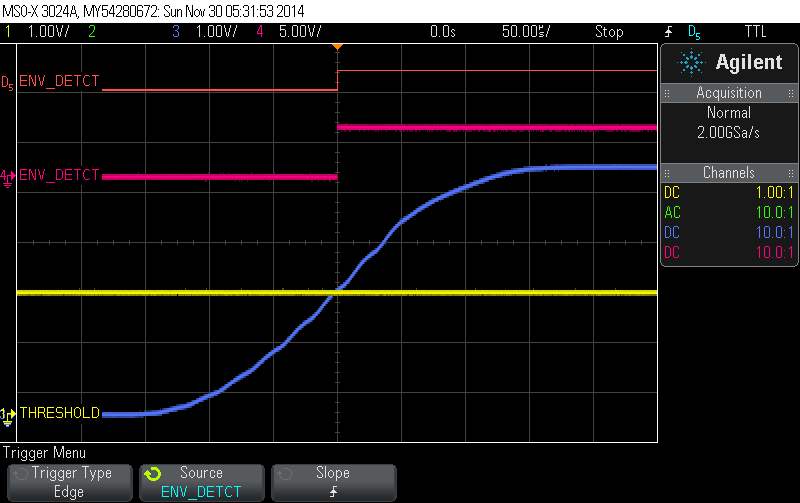
I’m using the same fast comparator for the envelope detector as for the ZCD. And it works just as perfectly here. Above you see how it generates a perfectly clean output signal (pink) when the envelpe (blue) crosses the threshold (yellow).
As you can see, there is still a small amount of ripple in the envelope. I have set the -3db points of the filters quite a bit higher than in the first version: 15k plus 1nF results in about 10.6kHz. So I’m smoothing the envelope quite a bit less than I used to.
I might try increasing the 100k resistor at the input to maybe 150k. That would result in less saw-toothing at the filter input (ENV1 above). But for now I leave it as it is.
Signal routing / multiplexer
I’m now using the second, otherwise unused half of the 74HC4052 to route the PWM signal to the right buffer of the 74HC126. This works flawlessly.
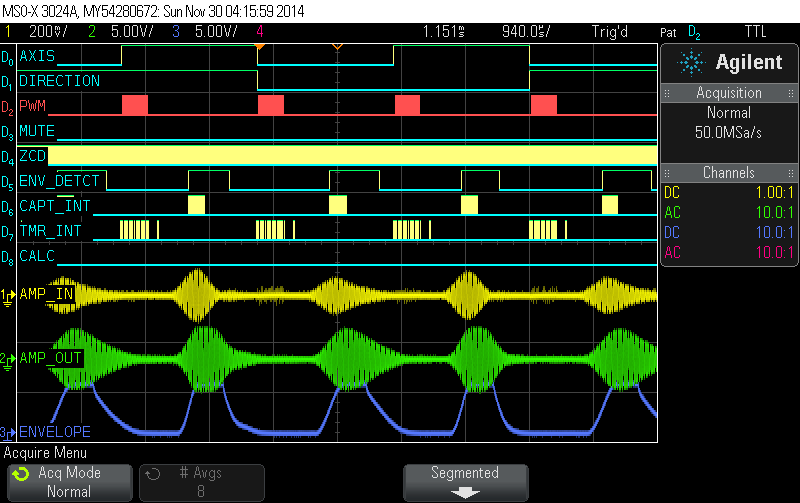
What doesn’t work is routing the pre-biased received signals to the amplifier. Well, the signal does get to the amplifier but look at the shape of the amplifier input (yellow signal) in the overview screenshot at the very top. It gets pulled down to zero every time I change the input channel.
So I had to change that back to how it was in the first version. The unbiased signal goes through the multiplexer and gets capacitively coupled into the amplifier where it is biased to the right level. But this time I don’t have the -5V supply at the multiplexer any more.
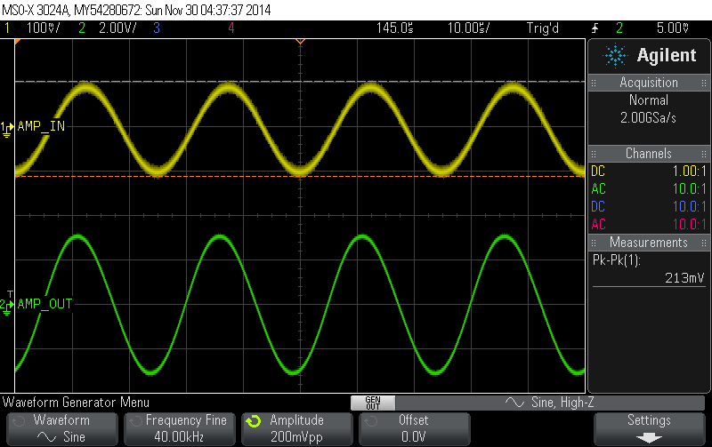
Here I’m again using a signal generator to generate an unbiased sine wave with 200mV amplitude pp which is applied at the multiplexer input. As you can see above, it reaches the amplifier input in perfect condition.
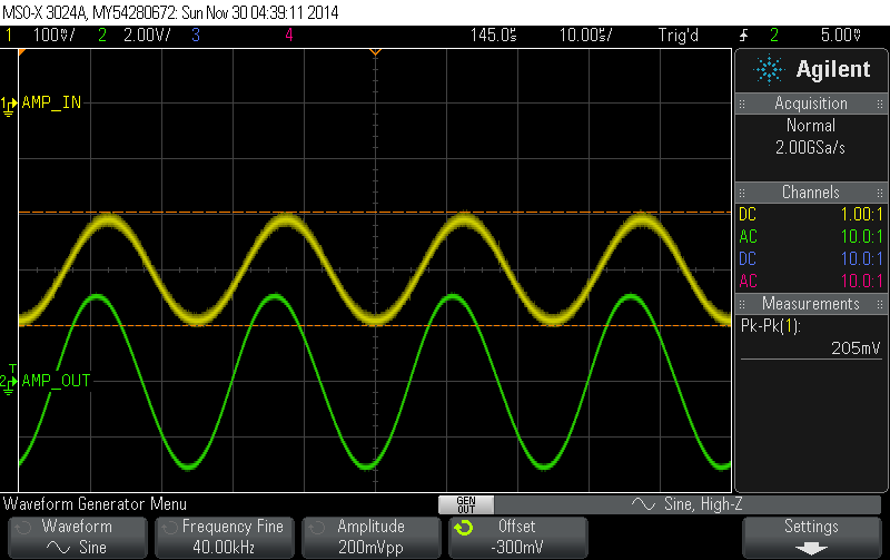
Even when I biased it to -300mV it passed almost unattenuated. Only when I increased the biasing to -700mV, the amplitude was cut in half:
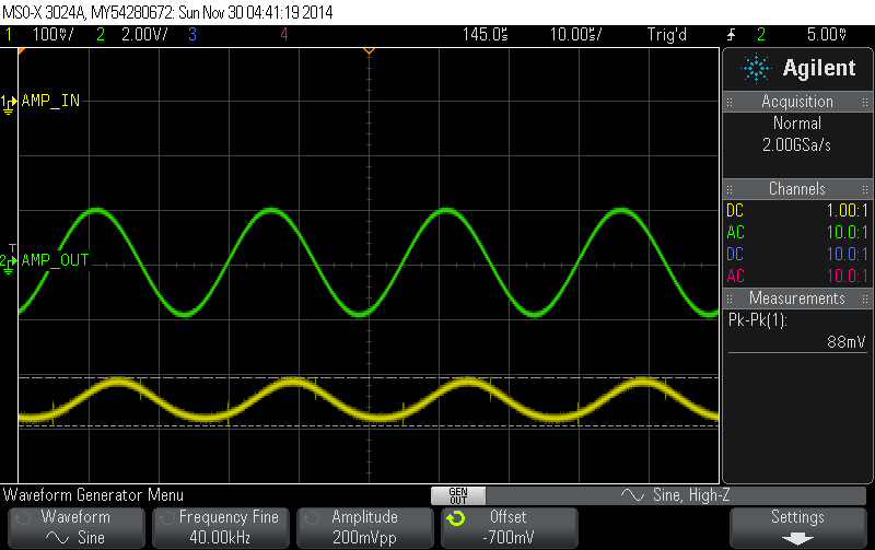
So I’ve replaced the four capacitors at the multiplexer inputs (C16, C24, C25, C26) with zero-ohms resistors and placed one of them at between the multiplexer and the amplifier input. For this second part I had to do a bit of surgery on the board but nothing major.
Now the amplifier input looks ok:
Crosstalk / Mute signal
I’ve eliminated two of the three multiplexers in this design and was prepared to get quite a bit of cross-talk because of that. This is why I planned ahead and included a mute signal that lets me mute both the amplifier input and output.
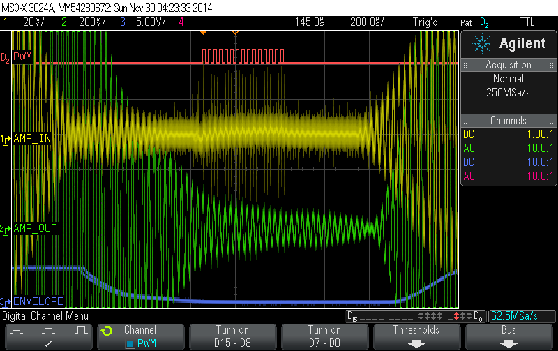
As it turned out, there was not much of a crosstalk problem. Yes, the received signal does pick up some (around 100mV pp) of noise from the transmitted signal but it doesn’t do much harm.
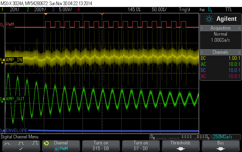
Most of the noise is high frequency spikes and they don’t make it trough the amplifier. Apart from that: We are never transmitting and receiving at the same time. Note that the screenshots above are with the mute signal disabled. So I probabely won’t use that mute functionality going forward. One singal less to worry about. And if I change my mind the circuit is still there.
Temperature sensor / Voltage reference
Not much of a surprise here. I’ve measured the voltage reference output at 2.4989 volts, very close to the rated 2.5V and well within specs.
The temperature sensor also works like advertised. But It seems to be significantly (several degrees) warmer than ambient. I’ve used a thermocouple to measure the temperature of the sensor and the board around it and really found it to be several degrees warmer.
I have placed it a bit close to the LED which heats it up a bit. The orange LED I’ve used turned out to be very efficient so it was very bright with the 330 ohms resistor. I’ve changed that resistor to 1k now and the LED is still quite bright and only consumes a third of the power. But it didn’t help much as far as the temperature sensor is concerned.
Seems the heat is not mainly coming from the LED. Which brings us to the next topic.
Power consumption
I’ve measured the current (at 12V) the arduino was pulling at its DC plug. Since the Arduino is using a linear regulator, current should be independant of input voltage. Anything above 5V is just disposed as heat.
These are my results:
- Arduino + shield + display: 67.3mA
- Arduino + shield: 61.0mA
- Arduino only: 52.4mA
So the display is pulling 6.3mA and the shield another 8.6mA. Most of the current is used by the Arduino itself.
The power consumption of the shield makes sense: Every darlington pair is pulling 1mA, the LED uses about 3mA. Makes 7mA so far which leaves 1.6mA for everything else.
The Arduino is using quite a bit more power than I thought. At 12V this makes about 0.6 watts. Which is probably what’s heating up our shield and the temperature sensor with it.
Summary
I’m quite happy with the new shield. After a bit of soldering everything is working fine. So from now on, this will mainly be a software project. Here’s an update on that: https://soldernerd.com/2014/12/04/arduino-ultrasonic-anemometer-part-12-working-on-an-arduino-library/

I don’t believe I see the changes discussed in this post in the PDF schematics available on the summary page. Is there a revised version forthcoming? I’m looking forward to attempting this project myself.
Hi Chad
You’re correct, the schematics do not yet reflect the changes. I’ve just made the changes and put a new version online. It’s on the project overview page under downloads Rev2.
I’m glad to hear you’re willing to give it a try yourself. Please be aware that I’ve never actually build this version yet so be sure to check it carefully before making one.
Regards
Lukas
Some more testing issues.
On my reproduction, I tried the first arduino sketch and it didn’t go well on the transmitting part as the signal was really not that great. The issue was with the fall time wich was way too long and so the 15 pulses overlapped. First, I suspected issues with the routing as the pcb has been rerouted in order to minimize the number of vias. I’m a newbie in pcb design but I don’t think I have to be carefull at 40 kHz and care about signal integrity, current loops, return paths and such.
Then, I tried the second version of the sketch, the one using the library and assembly code. And It was MUCH better. Clean 15 pulses at 40 kHz. Weird.