It’s been about one and a half years since I started out with my ultrasonic anemometer project. Like others before me I had to notice that this a much more demanding project than it appears to be at first. After countless hours of development and testing I have built this Arduino shield. It worked but the reliability of the measurements was never what I had aimed for. The problem was mainly how to figure out the absolute phase of the received signal. So the measurements were always precise – but sometimes off by a full wavelength. Then I was more or less inactive for most of 2015, mainly due to personal reasons. So the project was kind of stuck but i kept (and keep) getting a lot of encouraging feedback from you folks. I came up with new circuit ideas and decided to pretty much start with an entirely new design and to re-think each and every design choice I had made back then.

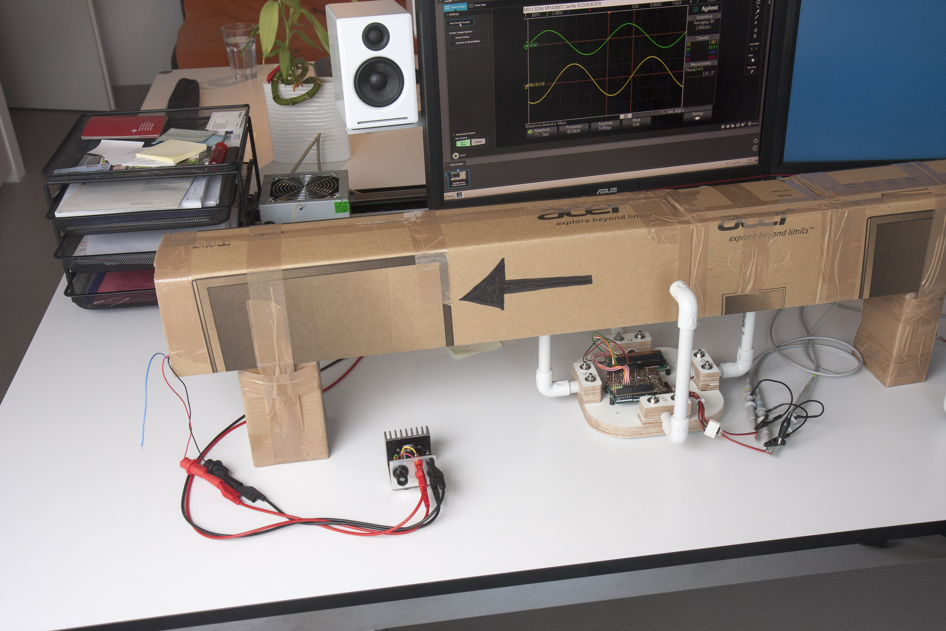
I will now outline and explain my new design for the send/receive circuit. So the board we are looking at today will handle the signal routing from the microcontroller to the individual transducers and from the transducers back to the amplifier where it is cleaned-up and amplified. There’s the circuit explained step by step.

Powerful 12V drive
My last design drove the transducers from a 74HC126 line driver / buffer. This chip has tri-state outputs which made it easy to switch to receive mode by releasing the respective transducer. It also has a strong (for a logic IC) output drive of up to 125mA to switch the capacitive load that the ultrasonic transducers present.
Unfortunately, the drivers only provided a 5V amplitude. Even worse, a more contemporary design would probably operate from a voltage of only 3.3 volts potentially making things worse in the future. So I decided to use a pair of Texas Instrument LM5111 Mosfet drivers. They can handle up to 18 volts so I can run them at a 12 volt input voltage directly. Mostet drivers are designed to drive large capacitative loads so they typically have powerful outputs. Specifically, the LM5111 can sink and source 5 and 3 amps, respectively. Thats more than any logic chip could ever provide. They also share a industry standard pin-out so they are easy to replace should the LM5111 not be readily available from your preferred supplier.

Discrete Mosfet Switches
The downside of using a Mosfet driver is that they lack the handy tri-state output. So I had to find another way to release the transducers for receive mode. Readily available integrated switches and multiplexers don’t have the low Rds-on that we need here. And they are definitely not happy if you’re trying to pass 5 amps through them. So I decided to use a discrete p-channel Mosfet for each transducer. With the gate at -5V the Mosfets conduct in the 0 to 12V range of the driving signal with a on-resistance of far below 1 ohm. So the strong drive of the LM5111 is not forfeited. With the gate at +5V the Mosfet is not conductive for signals a few volts around ground. So the receiving transducer can swing freely, unaffected by the LM5111.

Op-Amp Amplifier and Filter
The last design used a tuned two-stage common emitter amplifier. I found the design quite beautiful with nice biasing and everything but there were severe drawbacks. Mainly, the LC tank had to be tuned carefully to have it’s center frequency at 40kHz. Coils especially have large tolerances, plus/minus 20% is quite typical. This makes it at least difficult to produce any quantity of these things efficiently. It also takes some test equipment to see if your resonant frequency is correct so the design is not really suitable if you want to distribute it as a kit.
So this design uses a dual op amp at its center. I’ve decided to use a Texas Instrument LMC6482. This is an affordable precision OpAmp with rail-to-rail inputs and outputs that can run from a wide range of supply voltages. One of its main advantages for this application is its slew rate of 1.3 volts per microsecond. This is not especially much or especially little. But it’s just right for us. And this is why: A 40kHz signal with a peak-to-peak amplitude of 10 volts needs a maximum slew rate of 1.25 V/us. So 1.3 volts is enough when operating from a +/- 5V supply. And because it is just enough it will quite effectively block any high frequency noise/spikes that might be present at the input. This is a trick I’ve learned from Horowitz & Hill’s classic Art of Electronics. It’s my first time to use it so I’m exited to see how it works.
For now, the gain of the amplifier is controlled via a pot. Future designs will probably have a fixed gain once I’ve figured out how much gain we need.

Active Bandpass Filter
Just in case the slew rate limitation of the op amp isn’t enough to get a nice, clean output signal I have planned ahead and used the second op amp from the dual LMC6482 for an active band pass filter.
I’ve played around with an Excel spreadsheet and LT Spice for a few hours trying to find suitable values for the various resistors and capacitors. I’ll do some more experimenting once I can test the results on the real circuit. So don’t pay too much attention to the compoent values of this filter for now.

Signal Routing via 74HC4052 Dual 4-Channel Multiplexer
This is something that hasn’t changed much. The 74HC4052 has already been part of my last design. I’m now using two of them, one for transmitting and one for receiving.
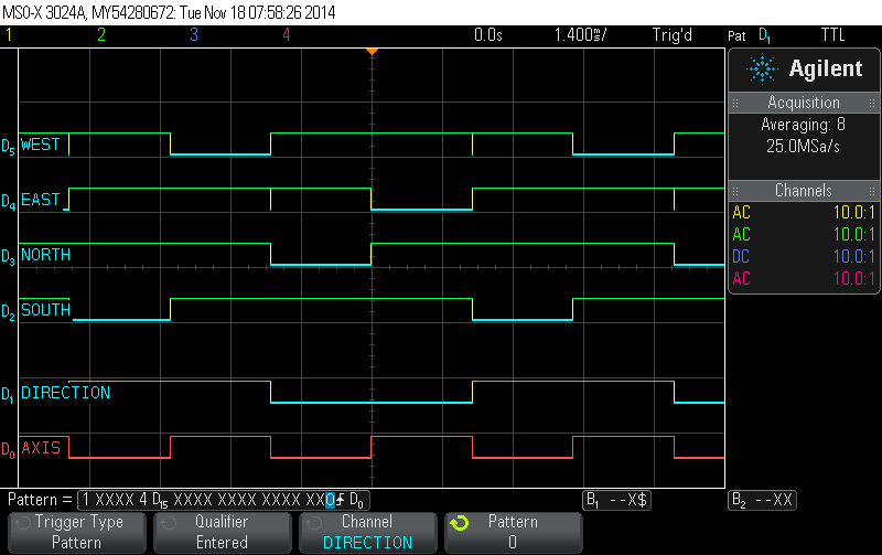
The first half of the transmitting multiplexer (IC2 in the schematic) takes the PWM signal from the microcontroller and sends it to the correct Mosfet driver according to the axis and direction signals that control which transducer is sending and receiving. The second half of that IC releases the receiving transducer located opposite of the transmitting one. It does so by providing +5V to the corresponding p-channel mosfet. Pull-down resistors to the -5V rail ensure that the mosfets are conducting when not actively turned off. The +5V release signal can be controlled from a microcontroller pin. Not sure if we need this functionality so a future version might just connect this signal directly to the positive rail.
The first half of the receiving multiplexer (IC1 in the schematic) routes the signal from the receiving transducer to the amplifier input. Note that there are 10k pull-down resistors on the floating leg of the transducers so the received signal is centered around ground. In order to avoid cross-talk, the second half of IC1 actively grounds the transmitting transducer’s signal. In order to make this possible, there are 10k resistors in the signal path before the multiplexer. Given the very hight input impedance of the op amp this should not have a negative effect.

Power Supply
This circuit runs from a 12V input voltage that is directly used for the mosfet drivers. For everything else, a linear regulator generates a +5V rail. An ICL7660 inverts this voltage to generate a -5V rail. The multiplexers and the op amp then run from this +/- 5 volt supply. This is somewhat of a complication compared to the sleek plus-five-volt-only approach that I took with the Arduino shield. But this gives us a much stronger 12V drive on the transducers even if a future design will run on +/- 3.3 volts. And the split supply allow for easy control of the discrete p-channel mosfet switches and ground referenced signals in the receiving circuit.

On-board Microcontroller
I’ve included a PIC16F1936 on the board. No, I don’t have any plans to use a PIC16 in my final design. I just thought it is convenient to generate the singals necessary for testing right on the board. I do consider using a dedicated on board microcontroller in my final design. I see several advantages of doing so. The design would no longer be Arduino specific. You could still interface it to an Arduino using a standard I2C or SPI interface. But you could also interface it to a Raspberry Pi or just about anything else. That would make it much more flexible and versatile. And even if you interface it to an Arduino the Arduino is free to focus on other things than handling the technical details of running the wind meter. With the shield one had to pay close attention not to upset the timing by running other code. So a design with an on-board chip would be easier to use as well. Cost would not really be an issue since powerful microcontrollers are available for around 2$ even in modest quantities. Feel free to share your thoughts on this. I’m currently looking at different architectures but no decision has been made yet.
This is it for now. In my next post I’ll share my test results with this circuit. The Eagle files and PDFs are available as a download on the project overview page. As always I very much appreciate your comments and suggestions.