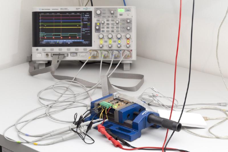
Last time I’ve presented my new design for the ultrasonic anemometer driver circuit. So now it’s time to see how it performs. If you’re new to this project you might want to check out the overview page or at least my last post.
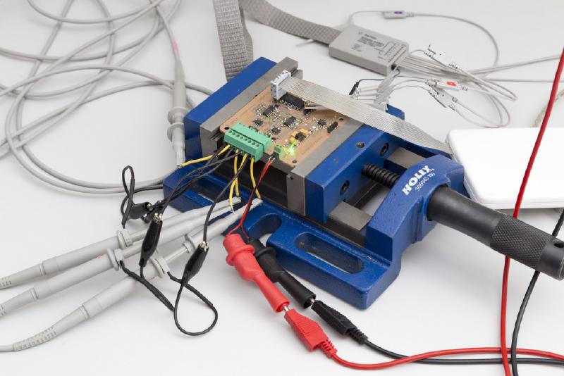
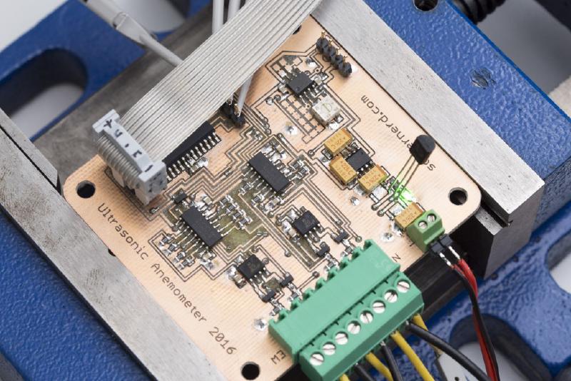
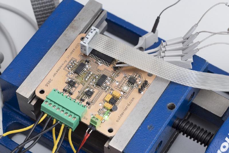
By now I had the time to build up the board and to do some testing. My main struggle was with the power supply. The linear regulator LM2931 comes in both fixed and variable voltage configurations. Unfortunately there is absolutely no way to tell them apart from their markings. So I accidentially used the variable voltage variant resulting in an almost 12 volts output voltage blowing up half of my circuit. I later noticed that I was out of 5V parts alltogether and had to use a LM7805 in a TO-92 package as you can see from the photo below.

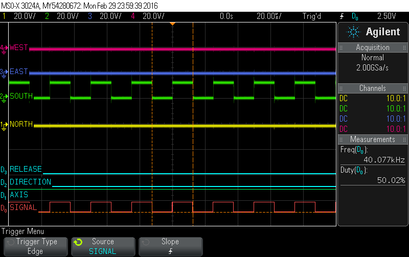
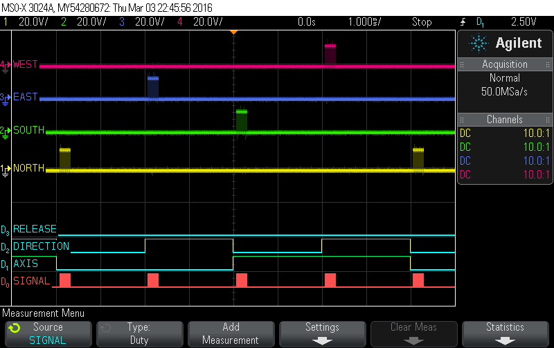
After having fixed the blown-up components, the circuit worked quite well. The first thing I did was to write some basic software for the PIC16F1936 to output a burst of40kHz PWM pulses every 2 milliseconds. After every burst the Axis and Direction signals are changed so the transducers take their turns in a clockwise order (North-East-South-West-…). The screenshot below shows part of such a burst sent from the South transducer. Note that the signal is a precise 40kHz with a duty cycle of 50% as it should be.
Below you see a full burst of 10 pulses. The number of pulses to send will be something to optimize in software once the hardware is finalized.
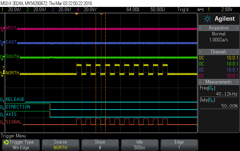
From the following screenshot you can nicely see how the transducers are selected by means of the Axis and Direction signals. The microcontroller always outputs its PWM burst from the same pin. All the signal routing is controlled by means of these two signals so there is not much of a software burdon.
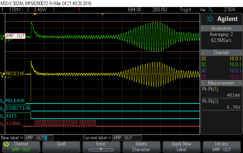
So sending pulses is easy and works well. But that’s the easy part. Now let’s see how the circuit performs in receiving and amplifying singals.
Below you see a complete send-receive cycle. A number of pulses is sent (red) and somewhat later received (yellow) and amplified (green). Notice the different scales. Despite being only slightly larger in amplitude on the screen, the ampified signal is about 15 times larger in amplitude. Remember from the last post that the gain is controlled by a pot so this is just a temporary setting.
The distance between the transducers is 230mm so the time delay should be roughly 700us. Looking at the screenshot below this seems to be the case.
Note that I’m sending much more pulses this time and that there is a larger-than-usual gap after the 18th pulse. As mentioned, I’m still experimenting with how many pulses should be sent and how. Here I’ve sent 18 pulsed plus 7 more pulses 180 degrees out-of-phase. My hope was that the received signal will decrease more rapidly in amplitude after reaching its peak which would make the peak easier to identify. This is still work in progress but I think this might be a simple way to improve the reliability of this wind meter.
Below you see an overview over a round of measurements. Note how different transducers produce different patterns. There seems to be quite a bit of manufacturing spread between them even though they are presumably from the same production lot.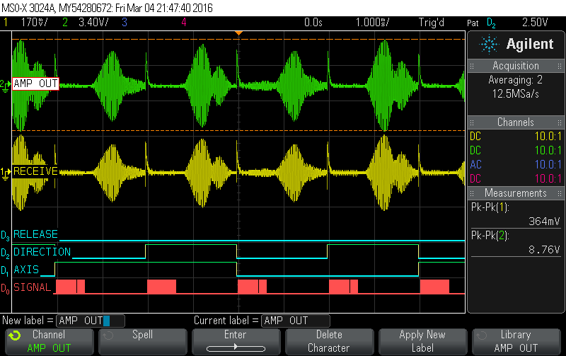
Now let’s look at these signals in a bit more detail. There is a significant amount of noise present in the received signal but it seems to be largely gone after the amplifier stage. The amplifier is a single op amp with a DC-coupled input and a pot acting as resistive divider setting the gain. That’s about as simple as it gets. There are no filters or anything up to this point. But the output looks nice and clean.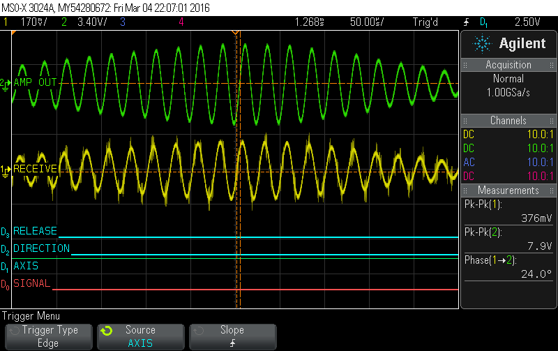
Here’s a close up making this even easier to see. There are narrow spikes present in at the input but the limited slew rate of the op amp seems to filter them all out. So the output is clean as a whistle without any filtering. Much better than expected. Wow.

If you’ve read my last post you know that there is a second op amp which I intended to use for a active band pass filter. But there seems to be no need for that at all. Simplifies the circuit, saves an op amp as well as quite a bit of board space. Great.
Nevertheless you might have noticed that there is a wider and much larger spike in the received signal every time the axis and direction signals change. The cause of this is most likely charge injection through the p-cannel Mosfets that are used as switches between the Mosfet drivers and the transducer.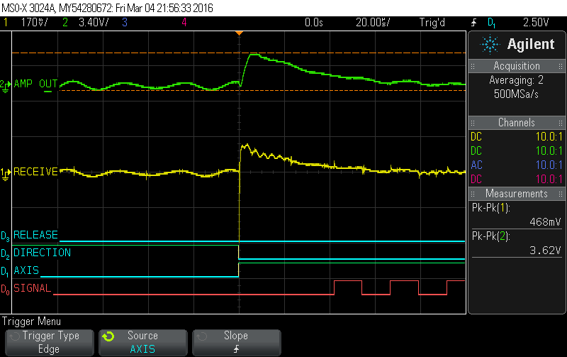
Being much slower and wider than the noise we’ve looked at so far, this spike makes through the amplifier with only slight attenuation. The good thing is that this spike occurs when we switch from one transducer to the next. That’s a time when we won’t want to look at the received singal anyway. We haven’t even sent any pulses yet. The spike abates long before the received singal starts being of interest. So I’m confident that this spike causes no real harm and can savely be ignored.
All in all I’m positively surprised how well this design has performed. I’m obviously getting a much stronger gate drive of 12 volts as opposed to 5 volts with my old design. And not only that. The Mosfet drivers used can source and sink several amps so there is reason to hope that the signal is not only larger in amplitude but also cleaner and more square. I’ll have to look at the shape of the wave form at the transducers in more detail to verify if this is really the case.

But I’m most surprised of how well the simple op amp performs. Using this super-simple setup I’m getting an output signal that’s just as clean as what I got from the rather complex two-stage tuned common emitter amplifier. No need to tune this thing making it much more production friendly. And it saves plenty of board space as well.
So this is the way to go I think. The next step will be to come up with some circuitry to process the received and amplified signal. I have some ideas in my mind and will elaborate on them shortly. But first I’ll take a closer look at the new lasercut mechanical design.